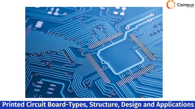
What is a Printed Circuit Board?
A printed circuit board is nothing but a printed wiring board which is a sandwich structure of conductive and insulating layers having a pattern of traces planes and other features. It is a backbone for almost all electronic devices which provides both mechanical support and electronic connectivity between different electronic components with the help of conductive pathways, pads and signal traces.
PCB devices are used in many electronic devices like smartphones and laptops (consumer electronics), medical devices, industrial machinery, and aerospace applications.
Types of Printed Circuit Boards
Single Sided PCB
Single sided PCB consists of a single layer of conductive material (typically made up of copper) mounted on one side of non-conductive substrate like FR4 (Fiberglass reinforced epoxy), phenolic or paper based materials.
This type of PCBs is very simple, cost effective and easy to manufacture. Their simplicity reduces the circuit complexity. This type of PCB is commonly used in consumer electronics, calculators, power supplies, LED lighting applications and basic sensors.
Double Sided PCB
Double sided PCBs consist of conductive layers on both sides of the substrate and because of this they are more complex. The electrical connections are established between two layers via the plated through holes.
They are widely used in various electronic devices like amplifiers, various control circuits, automotive dashboards, industrial controls and communication devices which makes a balance between affordability and circuit complexity.
Multilayer PCB
This type of PCB consists of three or more layers which are separated by insulating materials. They have high circuit density which enables complex designs in a smaller space. Multilayer PCBs are mainly found in smartphones, laptops, medical imaging devices, aerospace systems and high-speed computing applications.
Rigid Flex PCB
They contain both rigid and flexible sections in a single board. They are built on a solid, inflexible substrate, providing stability and durability. Rigid Flex PCBs can be single sided, double sided or multilayer, depending on the complexity of the application.
They are used in medical implants, military systems, aerospace avionics and wearable electronics where durability and compact circuitry is required.
Flex PCB
Flex PCB is a flexible PCB which is made from flexible materials such as polyimide or polyester. These boards allow the board to bend or twist without breaking it. These PCBs can also be single layer, double layer or multilayer.
These boards are lightweight and useful for applications which require compact and adaptable circuit designs. Because of their ability to fit into tight spaces, these PCBs are widely used in foldable smartphones, medical devices, automotive sensors and IoT devices.
Printed Flex PCB
In this type of PCB the conductive traces are printed directly onto the flexible substrate instead of being etched from copper. This technique reduces weight and manufacturing costs, making it ideal for disposable medical devices, smart textiles and RFID tags.
Metal Core PCB (MCPCB)
The base layer of this type of PCB is typically made up of copper instead of FR4. By effectively transferring heat away from critical components, MCPCBs prevent overheating. They are typically used in high power LED lightning, power converters, automotive electronics and industrial motor controllers.
Ceramic PCB
Instead of traditional fiberglass, ceramic PCB uses ceramic based substrates like aluminium oxide (Al2O3) or aluminium nitride (AlN). Because of their excellent thermal conductivity, electrical insulation and mechanical stability these PCBs are commonly used in aerospace, military radar systems, power electronics and high frequency applications where high heat resistance and durability are important
HDI PCB (High Density Interconnect PCB)
For achieving a higher density of components and interconnections within a smaller area HDI PCB has fine pitch microvias, buried vias and blind vias.
These PCB boards are used because they improve signal integrity, reduce electromagnetic interference (EMI) and enhance miniaturization. These PCBs are used in advanced medical equipment, high speed networking devices, tablets and smartphones.
UHDI PCB (Ultra High Density Interconnect PCB)
This type of PCB is an advanced version of HDI PCB which has features like fine circuit traces, smaller vias and increased layer density. This technology is very useful for cutting edge applications such as next-gen 5G and 6G communication devices, high frequency RF applications, AI processors and quantum computing systems.
Structure of PCB
For providing electrical connectivity and mechanical support for electronic components, printed circuit boards are composed of multiple layers which work together. Structure of PCB varies depending on its type but the fundamental elements remain the same.
1.Substrate (Base Material)
Substrate provides the mechanical strength and insulation for the circuit. For this they use materials like
FR4 (Fiberglass Epoxy) which is widely used due to its durability, heat resistance and electrical insulation properties
Polyimide (PI) or Polyester (PET) which allow bending and flexibility of PCB
Metal Core which is made of aluminium or copper is used to enhance heat dissipation in high power applications.
Ceramic which is made of aluminium oxide or aluminium nitride used for better thermal performance.
2. Copper Layer (Conductive Pathways)
Conductivity of electrical signals between components is carried out in the copper layer. Thickness of this layer is measured in ounces per square foot (oz/ft^2).
Single sided PCB has only one copper layer, double sided has copper layer on both sides and multilayer PCBs have multiple copper layers which are separated by insulating materials.
3. Solder Mask Layer
This layer acts as a protection for the copper traces to prevent oxidation, accidental solder bridges and short circuits. Mostly it is of green colour but it can also be red, blue, white or yellow. This layer ensures the enhancement of PCB durability and reliability.
4. Silkscreen Layer (Component Markings)
This layer is a printed layer which provides identification markings for component cables for resistors, capacitors and ICs, pin orientation indicators for correct placement of components and company logos, part numbers and manufacturing details. The main task of this layer is assembly of the PCB, troubleshooting and maintenance.
5. Inter Layer Connection (Vias)
For electrical connection between different layers, small holes are drilled into the PCB. There are different types of vias used in multi layer PCBs :
Through hole Vias used to extend through all layers of the PCB.
Blind Vias which connect an outer layer to an inner layer without passing through the entire PCB.
Buried Vias used to connect inner layers without appearing on the surface.
Microvias are used in HDI PCBs for high density connections.
6. Surface Finish
To protect the exposed copper pads and to improve solderability, surface finish is applied to the PCB. These include Hot Air Solder Leveling (HASL) which is cost effective, Electroless Nickel Immersion Gold (ENIG) which offers better durability and oxidation resistance.
Organic Solderability Preservative (OSP) which is environmentally friendly but has shorter shelf life and Immersion Silver which provides good conductivity and solderability but requires careful handling.
7. Electrical Components and Solder Joints
This is the final structure of PCB which includes assembling of various electronic components such as resistors, capacitors, ICs, diodes , connectors etc. These components are mounted by using Through Hole Technology and Surface Mount Technology.
How PCB are Design?
A well-designed PCB has qualities like efficient electrical performance, signal integrity, reliability and manufacturability. To design well PCB following steps are taken:
1. Design Requirement
Some design requirements are to be made before designing the PCB which includes
Board size and shape
Circuit Functionality - Decide the functionality of the PCB, whether power regulated, signal processing or communication PCB.
Layer count – single layer, double layer or multi-layer PCB
Power Requirement
Component Selection – Integrated Circuit, Wireless Modules, Relays, Diodes, Controllers
2. Schematic
Schematic design is to be made using different PCB design software like Altium Designer, Eagle, Ki-Cad, OrCAD etc. This includes:
Defining the connections after placing the electronic components.
Assignment of unique reference designators to each component (R1, R2, C1, C2, U1).
Power and ground connections for circuit stability.
To detect missing connections and errors, run an electrical rule check (ERC).
3. Layout Design
Physical placement of components and routing of electrical traces is takes place in that step:
Creating Board outline - Defining exact dimensions & shapes of the PCB and mounting holes are taken in that step.
Placing the components
Routing electrical traces
Via placement for Multi Layer PCBs
4. Electrical and Design Rule Check
Before finalizing PCB layout, ERC and DRC are checked by following ways :
Clearance Issues
Trace Width Violations
Unconnected Nets
Overlapping vias or pads
5.Generating Manufacturing and Gerber Files
After completion of PCB, files for assembly and fabrication are generated:
Gerber files - define copper layers, solder mask, silkscreen and drill holes.
Drill files
Bill of Materials (BOM)
Pick and Place file
6. Prototyping and Testing
PCB is manufactured and tested before mass production by electrical functionality, signal integrity, thermal performance and mechanical fitment.
7. Production and Assembly
Once a prototype is validated, PCB manufacturing and assembly is taken place by PCB fabrication, component assembly using SMT or THT technology, AOI and X-ray to detect soldering defects and final functional testing.
Applications of PCB
PCBs are used in consumer electronics products like smartphones & tablets, laptop & computers, television & smart displays.
They are used in automotive industries units like engine control units (ECU), infotainment systems, advanced driver assistance systems (ADAS), electrical vehicles (EVs) and lighting systems.
PCBs are also used in medical and healthcare devices. They are used in medical imaging devices (MRI, CT scan and ultrasound machines), patient monitoring systems(ECG devices), surgical equipment, hearing aids & implants and lab testing equipment.
PCBs are used in aerospace and defense systems for radar & satellite, missile & weaponry systems, drones & UAVs, space exploration equipment.
PCBs used in renewable energy and power generation systems like solar power systems (MCPCB), wind turbines, smart grid technology, battery management systems.
Printed Circuit Boards- FAQs
What are the different types of PCB materials?
Different types of PCB materials include FR4 (Fiberglass Epoxy), Polyimide, Metal Core (Aluminum, Copper), Ceramic (Alumina, Aluminum Nitride), PTFE (Teflon), and CEM (Composite Epoxy Material), each chosen based on thermal, electrical, and mechanical requirements.
What are the advantages of multilayer PCBs?
Multilayer PCBs offer high circuit density, improved signal integrity, reduced EMI, compact size, enhanced durability, and better power distribution, making them ideal for advanced electronic applications.
How to choose the right PCB thickness for a project?
Choose the right PCB thickness based on electrical requirements, mechanical strength, layer count, impedance control, thermal management, and manufacturing constraints, typically ranging from 0.2mm to 3.2mm.
What are the basic design rules for PCB layout?
Basic PCB layout design rules include correct trace width and spacing, proper component placement, ground and power plane optimization, minimal EMI, controlled impedance for high-speed signals, and adherence to manufacturing tolerances.
What is the cost factor in PCB design and manufacturing?
PCB design and manufacturing costs depend on layer count, material type, board size, trace complexity, via types, surface finish, assembly method, and production volume.

