What is P-Type Semiconductor?
If a trivalent impurity (for instance, Boron, Aluminium) is incorporated into an intrinsic semiconductor then it will, in turn, produce a more significant amount of holes on the valence band. Such types of semiconductors are called P-type semiconductors. When a trivalent impurity is introduced in a semiconductor, one of its three valence electrons makes covalent bonds with three neighboring atoms, while one bond lacks an electron.
For this reason, a vacancy exists that functions as a hole that seeks out electrons. The number of holes (nh) now exceeds the number of electrons (ne). Thus, in the case of p-type semiconductors holes are the major charge carriers whereas electrons are the minority charge carriers.
Formation of P-Type Semiconductor
The preparation of a semiconductor P-type is realized through the following steps:
Base Material
For this purpose take a pure intrinsic semiconductor known as germanium or silicon. This crystalline material consists of atoms in a lattice where each atom forms four covalent bonds with four valence electrons which are shared with other atoms.
Doping with Trivalent Impurities
Trivalent impurity is doped to a pure intrinsic semiconductor, for example, bore (B), aluminium (Al), gallium (Ga), or indium (In). Such elements have three electrons in their valence shell.
Holes
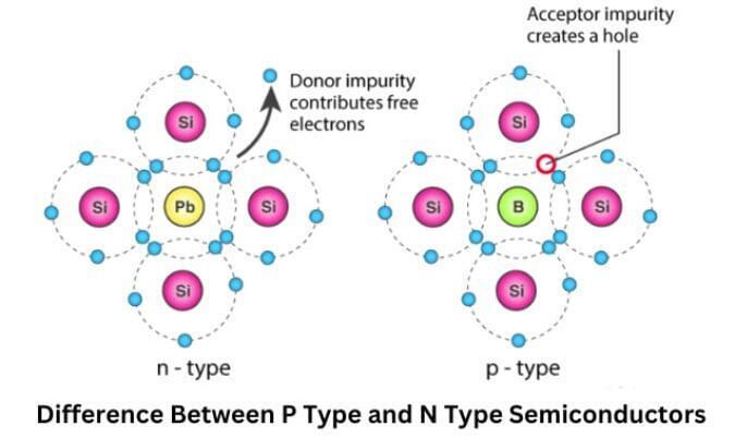
If boron or some other trivalent atom substitutes one atom of silicon or germanium within a crystal lattice, this means that the boron atom will establish three out of four covalent bonds with neighbouring tetramers but one out of four electrons cannot be bonded anymore since it is not available, and this absence of an electron creates a so called `hole’ or vacancy which can be accounted for as a positive charge carrier within the semiconductor.
What Is N-Type Semiconductor
To create an N-type semiconductor the process begins with a pure form of semiconductor such as silicon or germanium. Following this a small amount of a substance that has five valence electrons is introduced into it. In ensuring this action they create an environment rich in free electrons. It's these additional electrons that give the material its superior ability to conduct electricity.
Formation Of N-Type Semiconductor
When creating an N-type semiconductor there are specific steps one must follow:
Step 1:
Start off by picking a basic semiconductor such as silicon or germanium These substances stand out due to their even structure marked by a matching count of electrons and holes
When one mixes a substance with impurities that have five values :
Introduce an element with a pentavalent nature similar to phosphorus arsenic or antimony Elements like these carry five valence electrons offering one more than the needed four for bonding in the structures of silicon or germanium
The process by which electrons are set free involves :
When an impurity is present four valence electrons take part in creating covalent bonds with the surrounding atoms. As for the fifth electron it finds itself free to roam within the crystal structure. In this role it carries a negative charge which significantly enhances the flow of electricity.
Difference Between N-Type & P-Type Semiconductors
Feature | N-Type Semiconductor | P-Type Semiconductor |
Doping Element
| Doped with pentavalent impurities (e.g., phosphorus, arsenic) | Doped with trivalent impurities (e.g., boron, aluminum) |
Charge Carriers
| Electrons (negative charge carriers)
| Holes (positive charge carriers)
|
Majority Charge Carriers | Electrons
| Holes
|
Minority Charge Carriers | Holes
| Electrons
|
Conduction Type
| Electrical conduction primarily due to electron movement
| Electrical conduction primarily due to hole movement
|
Fermi Level Position
| Closer to the conduction band
| Closer to the valence band
|
Electrical Properties
| Higher electron mobility, making it efficient for conduction
| Lower hole mobility compared to electron mobility
|
Energy Band Diagram
| Fermi level lies near or within the conduction band
| Fermi level lies near or within the valence band
|
Application
| Used in diodes, transistors, solar cells, and integrated circuits
| Used in diodes, transistors, solar cells, and integrated circuits
|
Example Materials
| Silicon doped with phosphorus or arsenic
| Silicon doped with boron or aluminium
|
Behavior in a PN Junction
| Electrons move from the N-type region to the P-type region, forming a depletion region
| Holes move from the P-type region to the N-type region, forming a depletion region
|
Final thoughts
N-type and P-type semiconductors are extremely important parts of electronic technology with their own unique features that make them useful in semiconductor devices. N-type semiconductors have extra electrons , making them great for tasks that need fast-moving electrons and good conductivity. On the other hand, P-type semiconductors have fewer electrons, creating holes, which allow positive charges to move.
The way these two types of semiconductors work together is key to making basic components like diodes, transistors, and solar cells. These parts are crucial for how electronic circuits and devices function. To really understand how semiconductors work and their role in new electronic developments, it’s important to know the differences between N-type and P-type semiconductors.
FAQs on P and N Type of Semiconductor
1 . Can a P-type semiconductor be converted to N-type semiconductor?
Yes, a P-type semiconductor can be converted to an N-type semiconductor by doping it with a sufficient concentration of pentavalent impurities.
2 . What are the challenges in manufacturing p-type semiconductor and N-type semiconductor?
The challenges in manufacturing P-type and N-type semiconductors include achieving precise dopant concentration, maintaining crystal lattice integrity, and avoiding contamination during the doping process.
3 . What is the role of semiconductors in electronics?
Semiconductors control and regulate the flow of electrical current in electronic devices, enabling functionalities like switching, amplification, and energy conversion.
4 . What is the role of electrons in N-type semiconductors?
In an N-type semiconductor, electrons act as the majority charge carriers responsible for conducting electricity.
5 . What is the role of holes in P-type semiconductor?
The role of holes in a P-type semiconductor is to act as the majority charge carriers, enabling the flow of electrical current through the movement of electrons filling these holes.
6 . How does temperature affect P-type and N-type semiconductors?
Temperature increases the number of charge carriers (holes in P-type and electrons in N-type semiconductors), enhancing conductivity, but excessive heat can disrupt the semiconductor's properties.

